

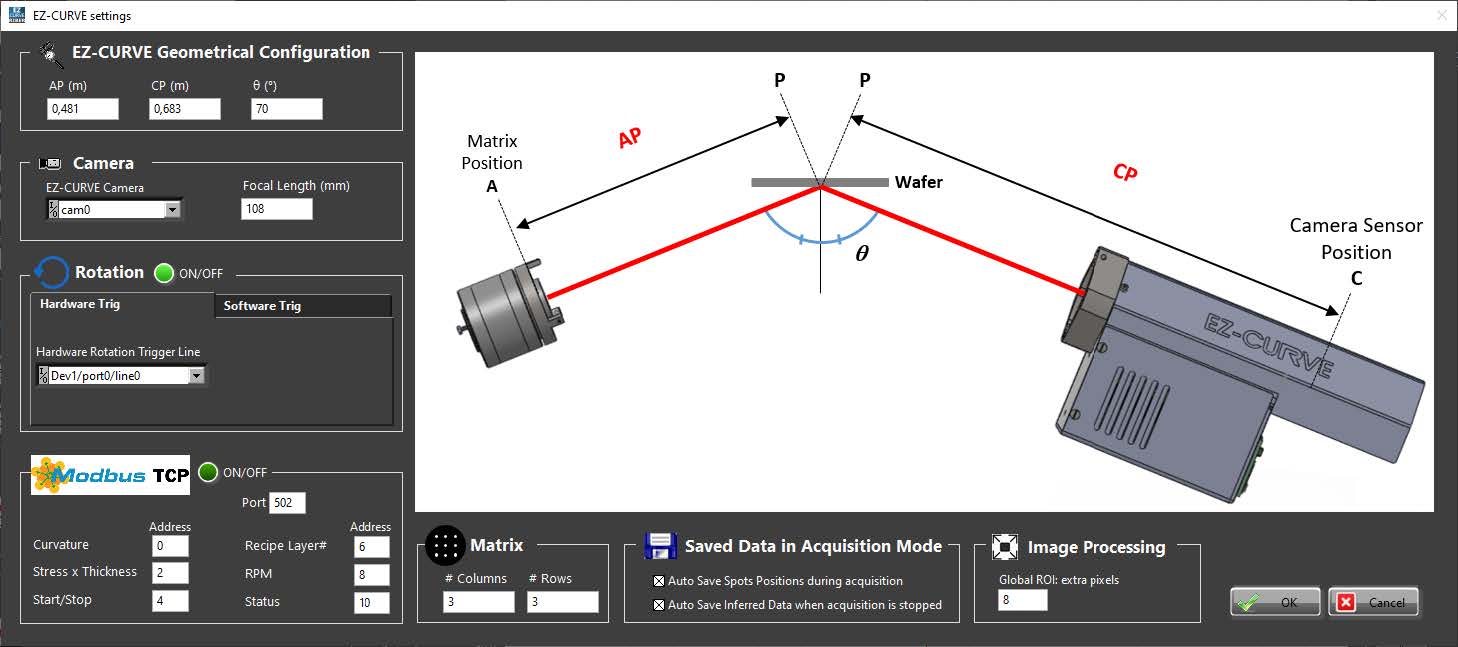
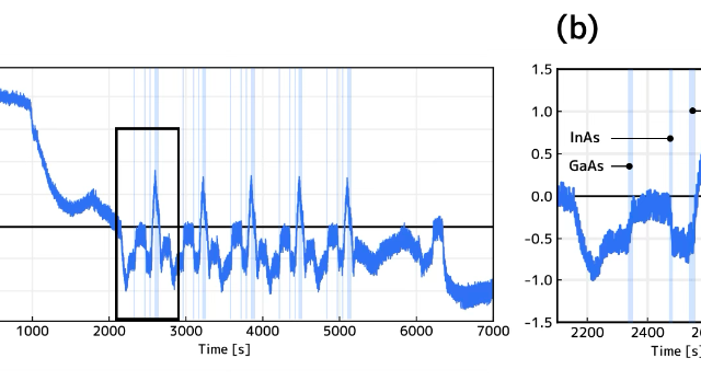
EZ-CURVE® is an in-situ stress, bow and curvature measurement tool, which enables access to these parameters in real time. It is based on Magnification Inferred Curvature (MIC) principle: a light pattern is projected onto the wafer; when curvature occurs, the image undergoes deformations, which amplitude give access to the curvature radius. With this instrument, it is possible to record precise growth patterns and then monitor any deviation which can occur from this reference in the following growths.
It also highlights specific growth events, thus enabling fundamental knowledge about growth mechanisms.
This technique is suitable for various thin films deposition techniques (CVD, MBE, PVD,…) and vacuum treatment process (plasma etching, annealing, quenching …), with unrivalled curvature sensitivity.
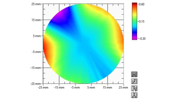
It gives access to complementary information, such as simultaneous spherical and cylindrical bowing or anisotropy measurement,
The technique is flexible: compatible with low lattice mismatch systems like AlGaAs/GaAs, with thick wafer (up to few mm), it is highly stable & alignment-free, it works over a wide-range of wavelengths, then being immune to reflectivity change and to wafer flatness
MY EZ-CURVE®
Create an account to access to “My EZ-CURVE®” and download the latest version of the software, the user manual and other resources.
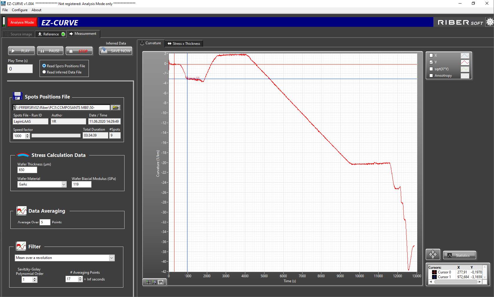
EZ-CURVE® Software
Discover EZ-CURVE advanced functions:
Curvature, Stress, Phase and Anisotropy measurement & display, Intuitive data acquisition, Powerful data saving functions, Real time mode up to 100 fps, Flexibility to share data with other, software incl. Riber Crystal XE, Post-processing and data treatment, Remote modbus interface
Main BENEFITS
- In situ stress, bow and curvature measurement, in real time
- Set precise growth patterns and monitor deviations
- Detect specific growth events and retrieve fundamental knowledge about growth mechanisms
- Suitable for various thin films deposition techniques (CVD, MBE, PVD,…) and vacuum treatment process (plasma etching, annealing, quenching …)
- Unrivalled curvature sensitivity
- Simultaneous spherical and cylindrical bowing, anisotropy measurement
- Compatible with low lattice mismatch systems like AlGaAs/GaAs
- Thick wafer compatible – up to few mm
- Highly stable & alignment-free measurement
- Wide-range wavelength source – immune to reflectivity change, no need to adjust exposure time
- Immunity to wafer flatness – possible use with patterned wafer

EZ-CURVE® publications
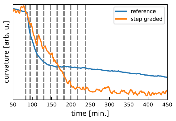
AlInAs step-graded buffer for reducing dark current in InAs based photodetector
Optics Express - 2025 - BARTŁOMIEJ SEREDYNSKI
Wide-range Emission Wavelength Control of InAs Quantum Dots by Changing Indium Composition in InAlGaAs Partial Capping Layer (2024)
Optica Open - 2024 - J.Kwoen

In situ monitoring of quantum dot growth using a magnification inferred curvature method (2024)
Applied Physics Letters - 2024 - J.Kwoen
